Research Home Research Objectives Team Members Reports Members Only
 
animation
Welcome!
Our objective is to enable nanophotonic components for communications and imaging systems by exploiting localized and propagating surface plasmons that access nanometer-scale wavelengths at optical frequencies.

This AFOSR MURI will create:

(a) a suite of plasmonic material designs

(b) comprehensive design and experimental realization of subwavelength component active and passive devices and small, circuit-like networks

(c) a toolbox of plasmonic network design methodologies.


Highlights

Click here for a poster highlighting the recent research of the Caltech Plasmonics MURI team (pdf)


News

bullet Gordon Research Conference
July 27-August 1, 2008
Tilton School, Tilton, NH

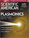
bullet Harry Atwater, Howard Hughes Professor and Professor of Applied Physics and Materials Science, has authored the cover article of Scientific American (April 2007) with his article "The Promise of Plasmonics." He describes the potential of technologies that use electron density waves called plasmons. Among many potential applications, plasmonic circuits could help the designers of computer chips build fast interconnects that could move large amounts of data across a chip. Read more...

bullet Meeting Calendar

bullet Nanometa 2007
The 1st European Topical Meeting on Nanophotonics and Metamaterials
January 8-11, 2007, Seefeld ski resort, Tirol, Austria. Click for details...


| News Archive |


California Institute of Technology | Harvard University
University California San Diego | University California Los Angeles

© Caltech | Last Update: November 30, 2007